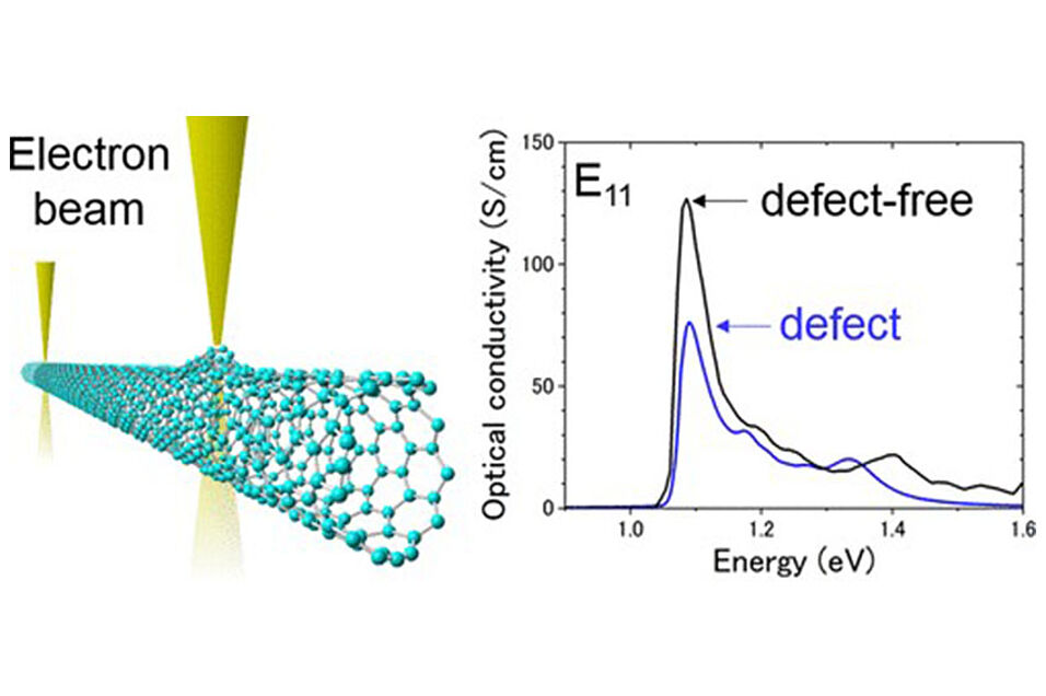
Measurements of optical properties at a nanometer level are extremely important but challenging using conventional light-probes. In a recent publication in Nano Letters a co-operation between scientists from AIST in Japan led by Ryosuke Senga and Kazu Suenaga and Thomas Pichler determined the absolute local optical conductivity at the gap transitions of a nanoscale semiconductor with separated defects using high resolution electron energy-loss spectroscopy as probe. This opens up a new ability to assign defect-related excitonic behaviors in semiconductors in optoelectronic devices, such as light-emitting diodes or solar cells and will be a crucial tool to optimize their performance.
Direct Proof of a Defect-Modulated Gap Transition in Semiconducting Nanotubes
Nano Lett., DOI: 10.1021/acs.nanolett.8b01284