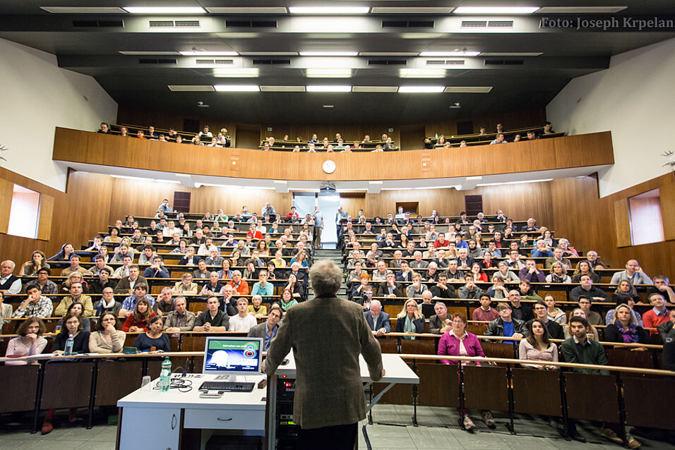
The materials that have enabled the information technology revolution over the past decades will soon reach their physical limits. Novel nanomaterials and technologies have therefore become a major focus of current solid-state research, with two-dimensional (2D) atomic crystals being one of the most promising candidates. Graphene, a 2D structure of carbon atoms with unorthodox electronic properties, is the most prominent representative of the 2D material family. More recently, transition metal dichalcogenides (TMDs) have come into the focus of interest, as these offer properties that complement those of graphene. Some TMDs are semiconductors with a sizable bandgap, which allows the construction of logic transistors, light emitters, photovoltaic solar cells, and other devices. In the first part of this talk, I will present some of our results on the development of 2D transistors and electronic circuits. Large-area MoS2 growth by chemical vapor deposition, together with the development of logic stages, enabled us to realize the first large-scale integrated circuit based on a 2D material – a basic microprocessor. I will then review our activities on photovoltaic energy conversion, photon detection and electrically driven light emission in TMDs. In particular, monolayer p-n junctions, formed by electrostatic doping of WSe2, and MoS2/WSe2 van der Waals heterojunctions will be presented. Upon optical illumination, conversion of light into electrical energy occurs in both types of devices. I will present measurements of the electrical characteristics, the photovoltaic properties, and ultrafast spectroscopic studies of the carrier dynamics. Finally, photocurrent generation studies in graphene and applications in optical communications will be presented. The focus of our work in this sub-field is on the 2D material integration into silicon chips for novel photonic integrated circuits. It is envisioned that the excellent material quality, combined with the advantages of 2D materials, such as flexibility, high mechanical stability and low costs of production, could lead to new electronic and optoelectronic technologies.
Thomas Müller (Vienna): 2D nanoscale electronics and optoelectronics
Location:
Related Files

Foto: Joseph Krpelan
